Pro_PainKiller
Software-Overclocker(in)
AW: Nvidia Pascal: Fertigung soll in 16 nm FinFET über TSMC laufen
In den Entwicklung-Labors von Nvidia sind seit geraumer Zeit (Q4/2014) lauffähige Vorserien GP100 16 nm FinFET GPU's zum testen und ggf. nachoptimierten der finalen Pascal GPU Layouts. TSMC Achieves 16nm FinFET+ Risk Production - Nvidia Talks Next Gen Geforce GPUs
“NVIDIA and TSMC have collaborated for more than 15 years to deliver complex GPU architectures on state-of-the-art process nodes,…….Our partnership has delivered well over a billion GPUs that are deployed in everything from automobiles to supercomputers. Through working together on the next-generation 16nm FinFET process, we look forward to delivering industry-leading performance and power efficiency with future GPUs and SOCs.” – Jeff Fisher, Nvidia
With this latest update from TSMC, I am personally starting to lean towards no 20nm GPUs. It just wouldn’t make sense for companies like Nvidia to adopt 20nm just a few months before 16FF+ starts volume production. What would make sense is for Nvidia to have an intermediary core (GM200 anyone?) and then ramp directly to 16nm FinFET Plus. As for AMD, their PR department is currently angling for the 4K Performance fight, where the R9 290X thanks to its 512 bit bus can hold its own against the Maxwell flagships.
>>> Hier geht es nur noch um die finalen Fertigung- & deren Fertigungskapazitäten, über den grössten Chip-Auftragsfertiger TSMC (Taiwan Semiconductor Manufacturing Company) der seit 1998 (Nvidia Riva TNT) GPU's für Nvidia fertigt - und wohl auch wegen dieser jahrelangen Erfahrung & guter Zusammenarbeit ausgewählt wurde - Samsung & GloFo, und Co. (meisst nur für SOC zu gebrauchen - haben da keine langjährige Erfahrung mit '600 mm2 Monster' GPU-Chips), hatten da wohl nie eine wirkliche Chance den DEAL für sich zu gewinnen!
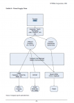
http://goodbadstrategy.com/wp-content/downloads/Nvidia.pdf /// NVIDIA Tapes Out "Pascal" Based GP100 Silicon | techPowerUp
In den Entwicklung-Labors von Nvidia sind seit geraumer Zeit (Q4/2014) lauffähige Vorserien GP100 16 nm FinFET GPU's zum testen und ggf. nachoptimierten der finalen Pascal GPU Layouts. TSMC Achieves 16nm FinFET+ Risk Production - Nvidia Talks Next Gen Geforce GPUs
“NVIDIA and TSMC have collaborated for more than 15 years to deliver complex GPU architectures on state-of-the-art process nodes,…….Our partnership has delivered well over a billion GPUs that are deployed in everything from automobiles to supercomputers. Through working together on the next-generation 16nm FinFET process, we look forward to delivering industry-leading performance and power efficiency with future GPUs and SOCs.” – Jeff Fisher, Nvidia
With this latest update from TSMC, I am personally starting to lean towards no 20nm GPUs. It just wouldn’t make sense for companies like Nvidia to adopt 20nm just a few months before 16FF+ starts volume production. What would make sense is for Nvidia to have an intermediary core (GM200 anyone?) and then ramp directly to 16nm FinFET Plus. As for AMD, their PR department is currently angling for the 4K Performance fight, where the R9 290X thanks to its 512 bit bus can hold its own against the Maxwell flagships.
>>> Hier geht es nur noch um die finalen Fertigung- & deren Fertigungskapazitäten, über den grössten Chip-Auftragsfertiger TSMC (Taiwan Semiconductor Manufacturing Company) der seit 1998 (Nvidia Riva TNT) GPU's für Nvidia fertigt - und wohl auch wegen dieser jahrelangen Erfahrung & guter Zusammenarbeit ausgewählt wurde - Samsung & GloFo, und Co. (meisst nur für SOC zu gebrauchen - haben da keine langjährige Erfahrung mit '600 mm2 Monster' GPU-Chips), hatten da wohl nie eine wirkliche Chance den DEAL für sich zu gewinnen!
http://goodbadstrategy.com/wp-content/downloads/Nvidia.pdf /// NVIDIA Tapes Out "Pascal" Based GP100 Silicon | techPowerUp
Anhänge
Zuletzt bearbeitet:
 Ich bezweifel sehr stark, dass sich jemand oberhalb einer 970 ernsthafte Gedanken machen muss, ob er zu nächsten Generation aufrüssten muss. Die großen Chips kommen sowieso erst später und werden sicherlich keine 980Ti oder Titan X in Grund und Boden spielen, wobei den den richtigen Enthusiasten egal sein dürfte, die rüssten sowieso auf.
") . Die Abkürzungen sind nicht zum Marketing gedacht, sondern benennen div. unterschiedliche Prozesse. Die Lxx Prozesse haben in der Regel ein PolySi Gate, während die S/Hxx ein HighK Metal Gate haben. Ausserdem unterscheidet sich das weitere Transistordesign je nach gewünschgter Taktrate.
. Die Abkürzungen sind nicht zum Marketing gedacht, sondern benennen div. unterschiedliche Prozesse. Die Lxx Prozesse haben in der Regel ein PolySi Gate, während die S/Hxx ein HighK Metal Gate haben. Ausserdem unterscheidet sich das weitere Transistordesign je nach gewünschgter Taktrate.") . Die Abkürzungen sind nicht zum Marketing gedacht, sondern benennen div. unterschiedliche Prozesse. Die Lxx Prozesse haben in der Regel ein PolySi Gate, während die S/Hxx ein HighK Metal Gate haben. Ausserdem unterscheidet sich das weitere Transistordesign je nach gewünschgter Taktrate.
. Die Abkürzungen sind nicht zum Marketing gedacht, sondern benennen div. unterschiedliche Prozesse. Die Lxx Prozesse haben in der Regel ein PolySi Gate, während die S/Hxx ein HighK Metal Gate haben. Ausserdem unterscheidet sich das weitere Transistordesign je nach gewünschgter Taktrate.


 Ich möchte diese mal in agschon sehen!