AW: AMD: Börsenanalysten halten Übernahme durch Microsoft für unrealistisch
AMD's Markt-Kapitalisierung (Börsenwert) war dieses Jahr bei 1.2 Milliarden USD, bei einem Jahrestiefst-Kurs von 1.61USD nach der Q2/2015 Quartalszahlen Bekanntgabe Ende Juli.
Wie schlecht es um AMD steht (AMD Verschuldung von über 2,2 Milliarden USD), zeigen die miserablen fundamentalen Kennzahlen & Börsenindikatoren.
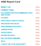
David Dreman Guru Analysis of Advanced Micro Devices, Inc. (AMD) - NASDAQ.com
EARNINGS TREND: [FAIL]
A company should show a rising trend in the reported earnings for the most recent quarters. AMD's EPS for the latest quarter is not greater than the prior quarter, (from earliest to most recent quarter) -0.23, -0.23. Hence the stock fails this test, but the investor should evaluate this company qualitatively to see if it qual ifies under this methodology's "exception rule".
RETURN ON EQUITY: [FAIL]
The company should have a high ROE, as this helps to ensure that there are no structural flaws in the company. This methodology feels that the ROE should be greater than the top one third of ROE from among the top 1500 largest cap stocks, which is 16.57%, and would consider anything over 27% to be staggering. The ROE for AMD of -393.33% is not high enough to pass this criterion.
LOOK AT THE TOTAL DEBT/EQUITY: [FAIL]
The company must have a low Debt/Equity ratio, which indicates a strong balance sheet. The Debt/Equity ratio should not be greater than 20%.
AMD's Total Debt/Equity of 1213.37% is not acceptable.
Nvidia hingegen, hat eine Markt Kapitalisierung von
12.4 Milliarden USD, satte 4.64 Milliarden USD free cash-flow / Bargeld-Reserven & keinerlei dept. / Verschuldung und seit 2012 einen stetig steigenden Aktienkurs von aktuell 23 USD. Analysten bewerten Nvidia (GP100/104 neue Pascal HBM2 GPU für HPC, High-Performance-Computing und Gaming Sektor) mit einem
Kursziel von 30 USD Ende 2015.
NVIDIA Pascal GPU Will Be Manufactured on TSMC 16nm FF Node - Flagship Single Chip Card To Feature 16 GB HBM2 VRAM
TSMC’s 16FF+ (FinFET Plus) technology can provide above 65 percent higher speed, around 2 times the density, or 70 percent less power than its 28HPM technology. Comparing with 20SoC technology, 16FF+ provides extra 40% higher speed and 60% power saving. By leveraging the experience of 20SoC technology, TSMC 16FF+ shares the same metal backend process in order to quickly improve yield and demonstrate process maturity for time-to-market value.
According to industry sources on Sept. 15, Nvidia decided to let TSMC mass produce the Pascal GPU, which is scheduled to be released next year, using the production process of 16-nm FinFETs. Some in the industry predicted that both Samsung and TSMC would mass produce the Pascal GPU, but the U.S. firm chose only the Taiwanese firm in the end. Since the two foundries have different manufacturing process of 16-nm FinFETs, the U.S. tech company selected the world’s largest foundry for product consistency.
The reason for Samsung’s determination to win the contract for the Pascal GPU lies in the fact that Nvidia’s new GPU is highly likely to mark a milestone in the next-gen graphic market. Experts are saying that Samsung’s failure to obtain the contract is mainly attributable to its lack of experience. The fact that the Korean tech giant has become TSMC’s rival only two years after it started to produce GPUs itself is considered to have special meaning at the moment.


 Dir ist aber schon aufgefallen, dass sie eine von insgesamt nur 2 Firmen sind, die diskrete Grafikkarten bis in den Highend-Bereich fertigen? Und dass AMD da momentan einen gewissen technologischen Vorsprung vor Nvidia hat (HBM ein Jahr früher eingesetzt, die GPUs unterstützen Asynchrone Shader, etc...)? Vor diesem Hintergrund erscheint die Aussage, dass AMD nichts hätte, und niemand Interesse daran hätte, wie Satire. Ich hoffe einfach mal, so war es auch gemeint